Language

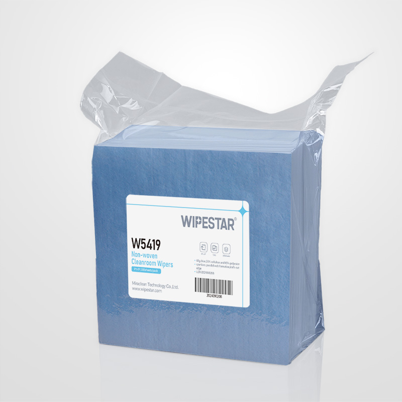
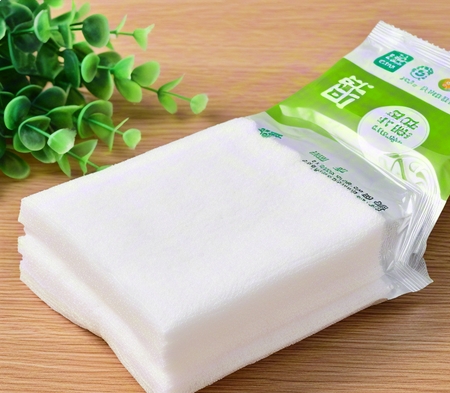
In the fields of precision electronic manufacturing and optical technology, a clean production environment has become the core element that determines product quality. As a dust-free wipe cloth for key consumables, with its unique material characteristics, it effectively solves the problems of surface cleaning and process pollution control of precision components. Below we will analyze the core values and technical indicators of this type of special cleaning materials in depth.
[Why do precision manufacturing prefer dust-free wipes?] Modern semiconductor wafer manufacturing requires no more than 10 particles per cubic meter of air (ISO Level 1 Cleaning Standard), which requires cleaning tools to have ultra-low dust generation characteristics. The dust-free wipe cloth is treated with ultra-long polyester fibers and is treated with cold cutting process, and the edges are made of laser edge sealing technology to achieve zero fiber peeling. Taking a well-known 12-inch wafer factory as an example, after introducing high-end dust-free cloth, the product yield rate increased by 1.8 percentage points, saving more than US$3 million in annual costs.

[Precise design of materials science] High-quality dust-free wipes need to pass three major technologies:
1. Fiber structure: Use microfibers with a diameter of 0.11μm (equivalent to 1/200 of human hair)
2. Processing technology: composite manufacturing technology of hot melt composite + ultrasonic cutting
3. Post-treatment: 18 pure water cleaning processes ensure ion residues are less than 0.01μg/cm²
[Deep influence of cleanliness indicators] In TFT-LCD panel manufacturing, 1μm particles will cause pixel point defects. A panel company quality report shows that after using a dust-free wipe with a cleanliness standard, the screen bad point rate dropped from 0.15% to 0.03%. Cleanliness control needs to be focused on: • Inorganic pollutants: Metal ions can cause electrochemical migration • Organic residues: Hydrocarbons cause coating adhesion to decrease • Microbial contamination: bacterial metabolites corrode precision contacts

[System Engineering for Pollution Prevention and Control] The full-process control system established by advanced manufacturing enterprises includes:
Raw material testing: Perform ASTM F51 dust test
Process monitoring: Real-time monitoring of online particle counters
Personnel management: Anti-static clothing and airlock dust removal system
Packaging standards: Double-layer vacuum aluminum foil to block environmental pollutants
Taking lithography machine lens cleaning as an example, professional-grade dust-free wipes must meet the following strict requirements at the same time: surface friction coefficient
In the fields of semiconductor manufacturing and precision electronics, pollutant control is the core element that determines product yield. Metal ion migration phenomenon may cause the surface of the photomask to atomize, such as sodium ions in environments with humidity exceeding 45% will trigger the light scattering effect of the glass substrate. Experimental data show that when the copper particle concentration exceeds 5 ppm, the microcircuit line width shrinks to 0.13 micron stage may cause bridge short circuits to adjacent lines.
The effects of chemical pollutants on wafers are diverse: boron-containing compounds may cause gate oxide layer thickness deviation up to ±3Å, while phosphorus-based substances may cause abnormal doping concentration distribution during high-temperature annealing. Volatile organic pollutants (VOCs) form molecular deposition layers in a clean room environment, which specifically manifests as etching residues of 0.2-0.5 μm on the surface of the photomask. It is worth noting that the dielectric constant of macromolecular pollutants such as selenite can reach 3.9, which may cause the interlayer insulation resistance of integrated circuits to drop below 10^8Ω·cm.
In a dynamic working environment, particulate contaminants with a particle size of more than 0.1 μm may cause wear and loss of moving parts of microelectromechanical systems (MEMS). Taking the hard disk head as an example, the presence of 3 0.3μm particles per square centimeter may cause a 15% reduction in read and write accuracy. Therefore, the cleanliness test of dust-free wipes must comply with the IEST-CC1246D standard. The key indicators include the non-volatile residue (NVR) that must be less than 10μg/m² and the ion content should be controlled within 0.1μg/cm².
Tags:
RELATED RESOURCES
7 Questions on Selecting Ultrafine Dust-Free Wipes: Comparative Analysis of Ultrafine Fiber Cleaning
Comparative analysis of ultra-fine dust-free cloth and ultra-fine dust-free cloth: professional selection guid......
More
Dust-free wipe cleaning technology essential: key parameters to improve 300-hour maintenance cycle
In the advanced manufacturing quality control system, dust-free wipe cloth cleaning technology has developed i......
More
9.9Inch dust-free wipe size specification: How ISO standards reduce consumable costs by 30%
Clean room cleaning revolution: Decrypting the scientific design of 9x9-inch dust-free wipesHistorical evoluti......
More
Analysis of the core technology of dust-free pre-wipes: ISO certification + examples of cleaning per
Analysis of core technology of dust-free pre-wet wipes and cross-domain application practiceIn the high-end ma......
More
Related Products
Room 101, Building 1, Angeer Factory, No.4, Hetian Road, Shatian Community, Kengzi Street, Pingshan District, Shenzhen, Guangdong, P.R. China 518122
info@wipestar.com
+86-755-89616775
+86-755-89616773
Related Products
RELATED RESOURCES
7 Questions on Selecting Ultrafine Dust-Free Wipes: Comparative Analysis of Ultrafine Fiber Cleaning
Comparative analysis of ultra-fine dust-free cloth and ultra-fine dust-free cloth: professional selection guid.........
More
Dust-free wipe cleaning technology essential: key parameters to improve 300-hour maintenance cycle
In the advanced manufacturing quality control system, dust-free wipe cloth cleaning technology has developed i.........
More
WIPESTAR
微信官方公众号