Language


This article focuses on explaining how contamination affects device processing, performance, and reliability in semiconductor manufacturing. We will examine and explain these principles, analyze the main types and sources of contamination, and discuss clean room layout, contamination control procedures, and wafer surface cleaning technologies.
One of the primary challenges in early microchip manufacturing was contamination. The industry began with clean room technology initially developed for the aerospace industry. However, these techniques proved inadequate for large-scale chip manufacturing. Clean room technology had to evolve alongside chip development, with designs and densities advancing accordingly. The industry's growth capability has consistently depended on solving contamination issues for each generation of chips. What might have been a minor issue yesterday could become a critical defect in today's chip manufacturing.
Semiconductor devices are susceptible to various types of contamination. These can be classified into five major categories:
Particles
Metal ions
Chemical contaminants
Bacteria
Airborne Molecular Contaminants (AMCs).
Semiconductor devices, particularly integrated circuits with high density, are vulnerable to all these contamination factors. This sensitivity is primarily determined by small feature sizes and the thickness of deposited layers on the wafer surface. These dimensions extend into the submicron range. While a micron (μm) is an extremely small unit, it's commonplace in semiconductor manufacturing. Current device dimensions (feature sizes) are in the nanometer (nm) range. To put this in perspective, a human hair has a diameter of approximately 100 μm (as shown in Figure 1). Given these minute physical dimensions, devices are highly susceptible to particle contamination from workers, equipment, and processing chemicals (as shown in Figure 2). As feature sizes continue to shrink (as shown in Figure 3), allowable particle sizes must be controlled to even smaller dimensions.

Figure 1: Size Comparison: Human Hair vs. Semiconductor

Figure 2: Primary Sources of Semiconductor Device Contamination

Figure 3: Evolution of Semiconductor Feature Sizes Over Time
A rule of thumb is that particle size must be half the metal 1 half-pitch. The half-pitch is half the distance between adjacent metal lines and spaces. Particles located in critical device areas that destroy functionality are known as killer defects. These killer defects also include crystal defects and other process-induced defect issues. On any wafer, numerous particles are present. Some are of the killer variety, while others are located in less sensitive areas and cause no harm. The 2011 International Technology Roadmap for Semiconductors (ITRS) identifies that defects are increasingly tied to yield and development, with more sensitive defect and contamination detection tools being crucial for yield improvement and advancement in future technology nodes.
As discussed in our other article, semiconductor devices require controlled resistivity in the silicon wafer and doped N and P regions, as well as precise N-P junctions. These three characteristics are achieved by introducing dopants into the crystal and wafer. These intended effects only retain very small quantities of dopants. Unfortunately, certain electrically active contaminants in the wafer can alter device electrical performance characteristics, leading to performance degradation and reduced reliability parameters.
The contaminants causing these issues are known as Mobile Ionic Contamination (MIC). These are metal atoms present in ionic form in materials (as they carry charges). Furthermore, these metal ions are highly mobile in semiconductor materials. This mobility means metal ions can move within devices, causing device failure even after electrical testing and shipping. Unfortunately, the metals causing these problems (as shown in Figure 4) exist in most chemicals used with silicon devices. On the wafer, MIC contamination must be controlled to levels of 10^10 atoms/cm² or less.

Figure 4: Metal Ion Contamination
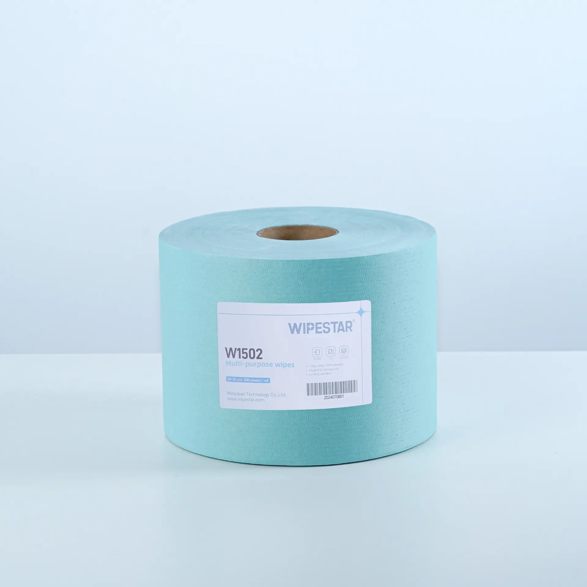
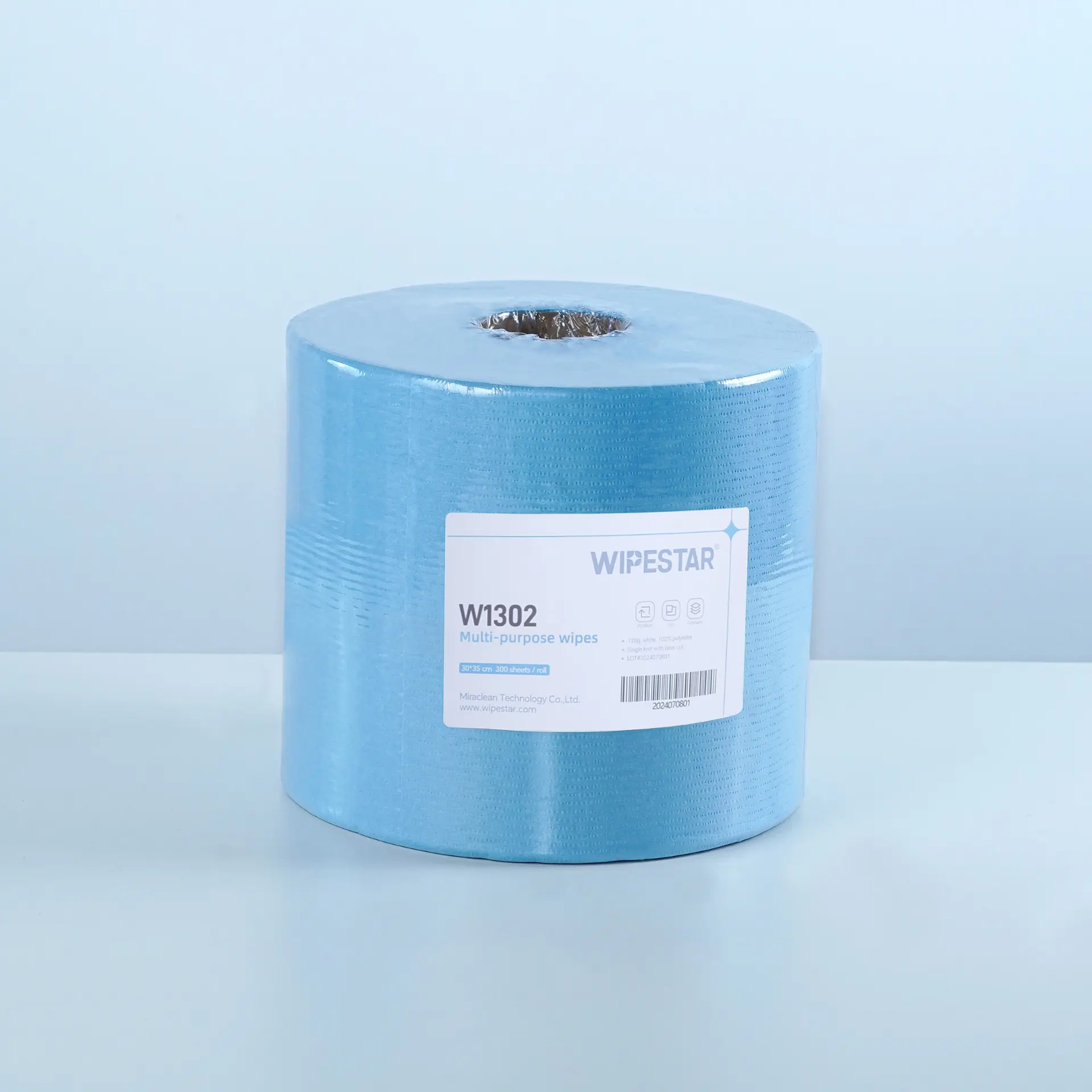
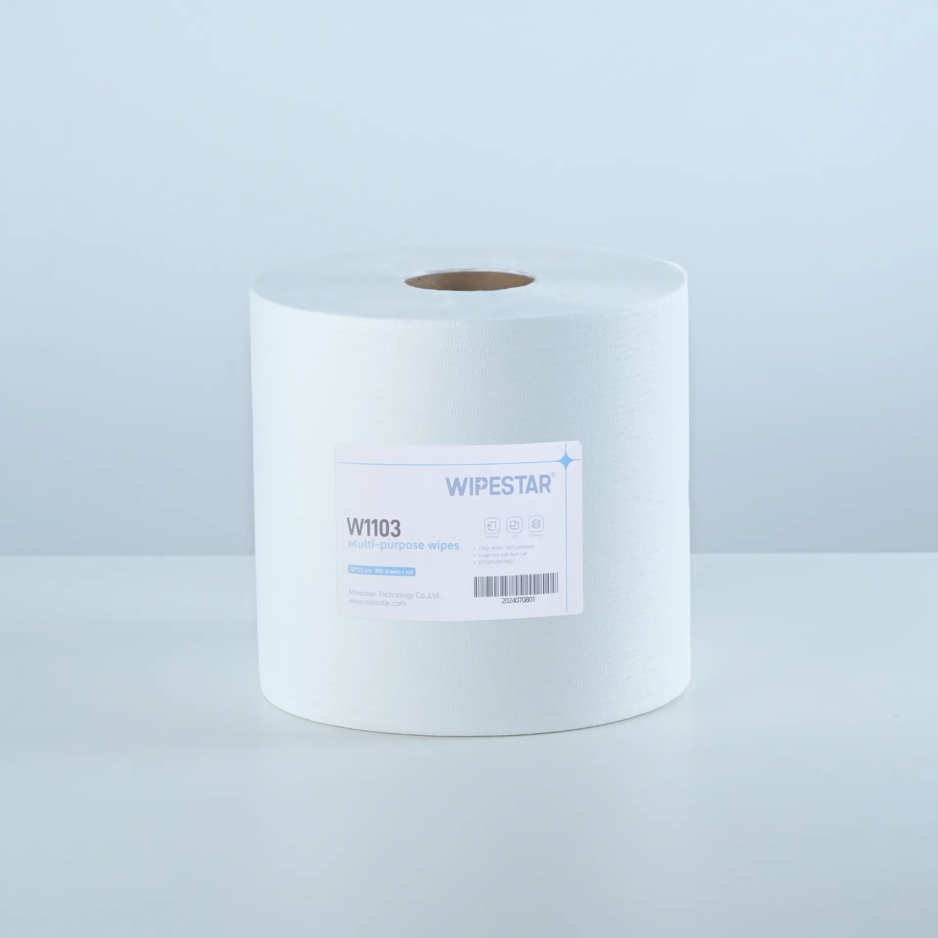
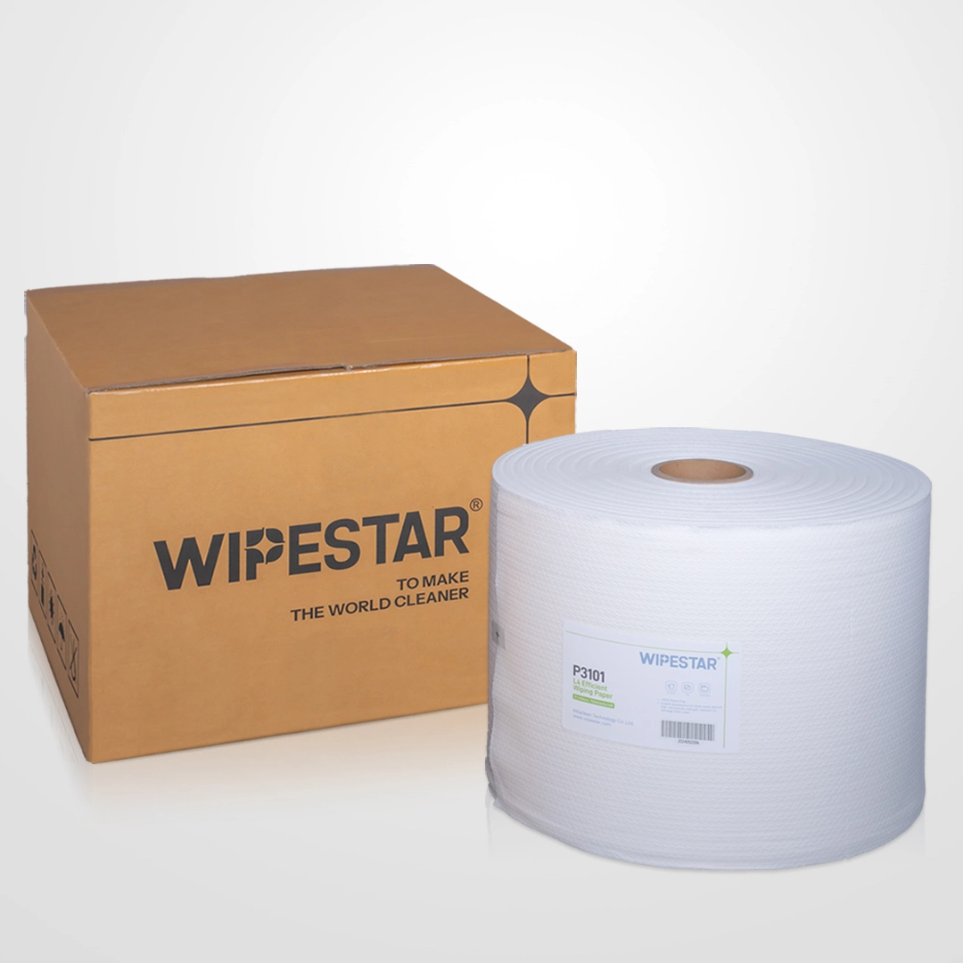
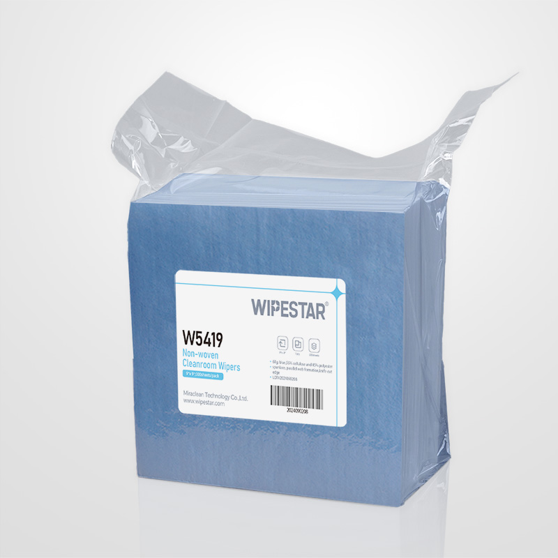
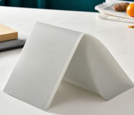
Wipestar Polyester Cleanroom Wipers deliver ultra-low particle generation essential for semiconductor manufacturing environments. Their 100% continuous filament polyester construction and precision edge treatments ensure superior cleanliness control during critical cleaning processes. Available in multiple specifications with laser, thermal or ultrasonic edges to meet your cleanroom requirements.
Everything You Need to Know about Cleanroom Wipers
Tags:Semiconductor
RELATED RESOURCES

How Aircraft Wipes Achieve Zero-Contamination Aircraft Engine Cleaning
Wipe star aviation-grade cleaning consumables are manufactured using innovative hydros pinning process, and th......
More
7 Questions on Selecting Ultrafine Dust-Free Wipes: Comparative Analysis of Ultrafine Fiber Cleaning
Comparative analysis of ultra-fine dust-free cloth and ultra-fine dust-free cloth: professional selection guid......
More
The difference between dust-free paper and wiping paper is revealed. 15 years of experience in the f
In the field of industrial cleaning consumables, dust-free paper and wipe paper are two core products often ca......
More
Clean room Wipes Buying Guide: 6 Key Indicators for Professional Purchasers.
Clean Room Dust-Free Wipe Cloth Selection Guide: A Decision Framework for Professional Procurement PersonnelIn......
More
Related Products
Room 101, Building 1, Angeer Factory, No.4, Hetian Road, Shatian Community, Kengzi Street, Pingshan District, Shenzhen, Guangdong, P.R. China 518122
info@wipestar.com
+86-755-89616775
+86-755-89616773
Related Products
RELATED RESOURCES
How Aircraft Wipes Achieve Zero-Contamination Aircraft Engine Cleaning
Wipe star aviation-grade cleaning consumables are manufactured using innovative hydros pinning process, and th.........
More
7 Questions on Selecting Ultrafine Dust-Free Wipes: Comparative Analysis of Ultrafine Fiber Cleaning
Comparative analysis of ultra-fine dust-free cloth and ultra-fine dust-free cloth: professional selection guid.........
More
WIPESTAR
微信官方公众号