Language


Electronic PCB Assembly (PCBA) cleaning, as one of the key processes in electronic assembly, has regained industry attention, particularly in the manufacturing of high-reliability products for military and aerospace applications. This renewed focus comes as assembly density and complexity continue to increase. To enhance electronic product reliability and quality, strict control of PCBA residues is essential, and in some cases, complete removal of these contaminants is necessary. This article systematically explores cleaning process theory and practice from manufacturing and OEM perspectives.
Electronic products consist of various electronic components assembled on printed circuit boards to form complete systems. The most fundamental assembly process is Printed Circuit Board Assembly (PCBA), where soft soldering (tin soldering) significantly impacts electrical performance and reliability. According to reliability analysis statistics from China CEPREI Laboratory's Reliability Research Center, failures during product use due to corrosion and electromigration-induced short circuits and open circuits account for 4% of issues, making them one of the major threats to product reliability.
In the past, cleaning received less attention primarily because electronic product PCBA assembly density was lower, and flux residues were considered non-conductive and benign, unlikely to affect electrical performance.
Today's electronic assemblies trend toward miniaturization, with smaller components and tighter spacing. Leads and pads are increasingly close together, creating smaller gaps where contaminants can become trapped. Even small particles remaining between two pads could potentially cause short circuits.
The fundamental reason QFN packages are prohibited in some high-reliability aerospace electronic products is that they lack leads that can buffer mechanical stress (such as PCB deformation). Instead, shear forces from PCB deformation are directly and repeatedly applied to the solder joints, leading to cracking.
In recent years, the electronics assembly industry has placed increasing emphasis on cleaning requirements, not only for product quality but also for environmental protection and human health. This has led to the emergence of numerous cleaning equipment suppliers and solution providers, with cleaning becoming a major topic in electronics assembly industry technical exchanges and discussions.
Contaminants are defined as any surface deposits, impurities, inclusions, or absorbed materials that reduce PCBA's chemical, physical, or electrical performance below acceptable levels. The main sources include:
Contamination or oxidation from the components and PCB materials themselves;
During PCBA manufacturing, solder paste, solder wire, and other materials used in the soldering process leave flux residues on the PCBA surface, which constitute the primary contamination;
Fingerprints from manual soldering, wave soldering claw marks, fixture imprints, and other surface contaminants such as via-hole plugging adhesive residues, high-temperature tape adhesive residues, fingerprints, and airborne dust;
Environmental contaminants including dust, water and solvent vapors, fumes, fine organic particles, and electrostatically-attracted charged particles that adhere to the PCBA.
These sources indicate that contamination primarily originates from the assembly process, especially during soldering.
During soldering, metals form a thin oxide layer when heated, which impedes solder wetting and affects the formation of solder joint alloys, potentially leading to cold or false joints. Flux serves a deoxidizing function, removing oxide layers from pads and components to ensure successful soldering. Therefore, flux is essential during soldering for forming good solder joints and achieving adequate plated through-hole filling.
In soldering, flux functions to remove oxides from PCB soldering surfaces to achieve necessary cleanliness, break surface tension of molten solder, prevent re-oxidation of solder and soldering surfaces during the process, and aid heat transfer to the soldering area. The main components of flux are organic acids, resins, and other ingredients. High temperatures and complex chemical reactions alter the structure of flux residues. The residues are often polymers, halides, and metal salts formed by reactions with tin-lead, which have strong adsorption properties but very poor solubility, making them more difficult to clean.
Contamination can pose direct or indirect risks to PCBA reliability. Organic acids in residues can cause corrosion. Ionized particles in residues can lead to electromigration between solder pads due to potential differences during operation, potentially causing short circuits and product failure. Residues can also affect conformal coating adhesion, leading to coating defects or failures. Some issues may not be immediately apparent but can emerge over time with temperature variations, causing coating cracks and delamination, ultimately leading to reliability problems.
Corrosion Case Study (See Figure 1)
Electron probe analysis revealed that besides carbon, oxygen, and tin-lead components, the solder joint surface contained abnormally high levels of halogen (Cl). These halogen ions, in the presence of air and moisture, create a cyclic corrosion effect on solder joints, eventually forming white, porous lead carbonate on and around the joints. Failed joints appear white and porous. In PCBAs using components with iron-based leads, the iron material, lacking complete solder coverage, quickly produces Fe3+ ions under the corrosive action of halogen ions and moisture, causing the board surface to turn red.

Figure 1: Corrosion
Additionally, in humid environments, acidic ionic contaminants can directly corrode copper leads, solder joints, and components, leading to electrical failure.
Electromigration Case Study (See Figure 2)
Ionic contamination on PCBA surfaces readily facilitates electromigration, where ionized metals migrate toward opposite electrodes and reduce back to metallic form, creating dendritic growth patterns (dendrites, whiskers). These dendrites can cause localized short circuits.

Figure 2: Formation of Electromigration Dendrites
PCBAs using silver-containing solders are particularly susceptible to electromigration after silver corrodes into ions. Interestingly, PCBAs that fail due to electromigration often return to normal functionality after proper cleaning.
Poor Electrical Contact Case Study (See Figure 3)
During PCBA assembly, resin residues such as rosin can contaminate gold fingers or other connectors. When PCBAs heat up during operation or in hot climates, these residues become tacky and attract dust or debris, increasing contact resistance or even causing open circuit failures. In BGA solder joints, corrosion of the PCB pad's nickel layer and the presence of a phosphorus-rich surface layer reduce the mechanical bond strength between the solder joint and pad, leading to cracking under normal stress and electrical contact failure.

Figure 3: BGA Solder Joint Cracking Leading to Electrical Contact Failure
PCBA contaminants are primarily bound through physical or chemical bonds. Physical bonds refer to molecular forces between contaminants and the PCB surface. These bonds are relatively weak, typically ranging from 0.8×10³ to 2.1×10⁴ J/mol. Rosin, resin, and adhesive residues are examples of physical bonding. Chemical bonds form when contaminants react chemically with the PCB surface, creating ionic or covalent compounds, such as metal resinates formed between rosin acids and metals. Chemical bonds are stronger, ranging from (4.2-8.4)×105 J/mol.
PCBA contaminants generally fall into three categories:
1. Polar Contaminants (also called inorganic contaminants, ionic residues, or ionic contaminants)
These substances can ionize into positively or negatively charged ions under certain conditions (when in solution), such as halides, acids, and their salts. Different ionic contaminants dissociate at different rates in various solutions.
In humid environments, when electronic components are powered, ions from polar contaminants migrate toward oppositely charged conductors, potentially forming dendritic metallic structures between conductors (such as between soldered leads). This reduces insulation resistance, increases leakage current between solder joints or conductors, and can cause short circuits.
Main types of ionic contaminants include:
Flux activators
Perspiration
Ionic surfactants
Ethanolamines
Organic acids
Plating chemicals
2. Non-polar Contaminants (also called organic contaminants or non-ionic contaminants)
These contaminants are non-conductive and act as resistors (insulators) on circuit boards, blocking or reducing current flow. Typical examples include rosin resin residues, wave soldering anti-oxidation oils, pick-and-place or insertion machine lubricants or waxes, tape residues from soldering processes, and skin oils from operators. These contaminants are sticky and attract dust. The organic residues (like rosin, oils) form insulating films that interfere with electrical contact between connector surfaces, switches, and relays. These effects worsen with environmental conditions and time, increasing contact resistance and potentially causing contact failure or open circuits. Sometimes rosin covering solder joints can interfere with testing, and non-polar contaminants can exacerbate contamination when combined with polar contaminants.
Main types of non-ionic contaminants include:
Rosin
Oils
Greases
Hand lotion
Silicone
Adhesives
3. Particulate Contaminants
Particulate contaminants typically include dust, smoke, lint, glass fibers, and electrostatically-charged particles from the work environment, as well as solder balls, beads, and dross from soldering processes. These can degrade electrical performance or cause short circuits, damaging electronic assemblies.
Particulate contaminants can be removed through mechanical methods such as high-pressure gas blowing, manual removal, or various cleaning processes.
1. Appearance and Electrical Performance Requirements
The most visible impact of PCBA contamination is on appearance, with residues potentially turning white due to moisture absorption in high-temperature, humid environments.
With the widespread use of leadless chips, micro BGAs, Chip Scale Packages (CSPs), and 0201 components, the spacing between components and circuit boards continues to decrease while assembly density increases. In fact, halides trapped underneath components or in areas inaccessible to cleaning can lead to catastrophic failures through halide release. This can also lead to dendritic growth, potentially causing short circuits.
Improper cleaning of ionic contaminants can cause numerous issues: reduced surface resistance, corrosion, and conductive surface residues forming dendritic patterns on circuit boards, leading to localized short circuits (see Figure 4).

Figure 4: Ionic Contamination-Induced Dendritic Growth Leading to Short Circuit Copy
For military electronic device reliability, tin whiskers and intermetallic compounds pose a significant threat. This persistent issue can ultimately cause short circuits. In humid environments under powered conditions, excessive ionic contamination can lead to problems such as electrolytic whisker growth, conductor corrosion, or reduced insulation resistance, resulting in circuit board trace shorts (see Figure 5).

Figure 5: Ionic Contamination-Induced Electrolytic Tin Whisker Growth Leading to Short Circuit
Inadequate cleaning of non-ionic contaminants can also cause various issues. These include poor solder mask adhesion, poor connector contact, physical interference with moving parts and connectors, and poor conformal coating adhesion. Additionally, non-ionic contaminants can trap ionic contaminants and other harmful substances within them, creating significant concerns that cannot be ignored.
2. Conformal Coating Requirements
For reliable conformal coating application, PCBA surface cleanliness must meet IPC-A-610E-2010 Class 3 requirements. Resin residues not removed before surface coating can cause protective layer delamination or cracking. Activator residues may lead to electrochemical migration under the coating, causing coating failure. Research shows that proper cleaning can increase coating adhesion by 50%.
3. No-Clean Also Needs Cleaning
According to current standards, "no-clean" means that board residues are chemically safe and can remain on the circuit board without adverse effects. Tests for corrosion, Surface Insulation Resistance (SIR), electromigration, and other specific tests primarily determine halogen/halide content to verify the safety of no-clean assemblies after completion. However, even low-solid content no-clean fluxes leave some residue. For high-reliability products, no residues or contaminants are permitted on circuit boards. For military applications, even no-clean electronic assemblies must be cleaned.
Cleaning is the process of removing contaminants, primarily using solution-based methods. It works by dissolving contaminants or breaking their physical or chemical bonds with the PCB through chemical reactions with the cleaning solution. Whether dealing with rosin, organic acids, or their tin or lead salts, all have some degree of solubility and can be removed through transfer from the board surface to the cleaning agent. The cleaning process can be enhanced by increasing cleaning agent temperature or using ultrasonic and brush cleaning techniques.
Post-assembly PCBA cleaning is a value-added process, primarily aimed at removing flux residues, tape adhesive residues, and other human-induced contamination to improve PCBA reliability. This was previously considered non-value-added work, which has proven to be an incorrect assessment.
PCBA cleaning includes both Surface Mount Technology (SMT) and Through-Hole Technology (THT) stage cleaning, which removes accumulated surface contaminants from various processing steps and reduces reliability risks associated with surface contamination.
When cleaning PCBAs, the first consideration is matching the cleaning agent with board assembly residues, particularly ensuring compatibility between flux residues and cleaning agents to achieve cleanliness targets effectively. An efficient cleaning process must ensure optimal matching of soldering temperature profile parameters, cleaning process parameters, and all parameters for solder paste and flux.
In wave soldering, potential reactions between post-reflow flux and solder mask can create dark stains, resulting in sticky contaminants that resist standard cleaning agents. Additionally, improper wave soldering temperature profiles, such as excessive preheat temperatures, can cause flux vitrification, preventing proper fluxing action and forming unacceptable contamination layers.
The chemical solvent cleaning process for removing flux soldering residues typically relies on alkaline pH cleaning agents containing metal ions. These metal ions promote chemical reactions forming lead salts, some of which (like Pb(NO)3) are water-soluble while others are not, potentially forming white precipitates on the PCBA surface.
With technological advancement and regulatory changes, cleaning products face increasing challenges. Standards like CEE 648 and REACH regulate which chemicals can or cannot be used in cleaning agents. In recent years, cleaning technologies using CFC, ETD, ES, and HCFC have been phased out, replaced by new chlorine-free solvents and water-based cleaning agents, along with new cleaning equipment.
From a cleaning capability perspective, Trichlorotrifluoroethane (CFC-113) was historically an ideal solvent, offering high degreasing efficiency, strong flux residue dissolution, easy volatility, non-toxicity, non-flammability, non-explosiveness, non-corrosiveness to electronic components and PCBs, and stable performance. However, it damages the atmospheric ozone layer, severely threatening human survival environments. Following the 1987 Montreal Protocol on Substances that Deplete the Ozone Layer signed in Montreal, Canada, the industry has continuously sought better alternative cleaning solvents to take over ozone-depleting substances (ODS). To date, no solvent has been found that completely matches CFC-113's superior cleaning capabilities.
Most small and medium-sized contract manufacturers or production facilities use manual brush cleaning methods due to cost considerations. This involves using an anti-static brush with cleaning solution to scrub the PCB held at a 45° angle, brushing from top to bottom to allow the dissolved residues to flow down with the cleaning agent. While this method is primarily used for spot cleaning or cleaning PCBAs with components that cannot be exposed to cleaning processes, it is inefficient and consumes large amounts of cleaning agent.
Major contract manufacturers and large production facilities are increasingly reconsidering their cleaning processes, implementing inline or offline cleaning machines to take over manual cleaning and ensure PCBA cleaning quality.
In practical cleaning processes, hand-soldered PCBAs often develop white surface residues after storage, with white marks prominently distributed around solder joints (as shown in Figure 6a), or wave-soldered PCBAs may show dark stains after cleaning (as shown in Figure 6b), severely affecting appearance inspection and failing to meet IPC-A-610E-2010 standards.

Figure 6a: After Storage Following Hand Soldering Clean

Figure 6b: After Cleaning Following Wave Soldering
White residues are common contaminants on PCBAs, typically flux by-products. Common white residues include polymerized rosin, unreacted activators, and reaction products between flux and solder such as lead chlorides or bromides. These substances expand when absorbing moisture, with some undergoing hydration reactions, making the white residue increasingly visible. These residues are extremely difficult to remove from PCBs, with problems worsening under prolonged heat or high-temperature exposure. Infrared spectroscopic analysis of PCB surface rosin and residues before and after soldering confirms this process.
Whether boards show white residues after cleaning, no-clean boards develop white substances during storage, or white substances appear on solder joints during rework, there are four main scenarios:
1. Flux Rosin: Most white substances appearing after incomplete cleaning, storage, or solder joint failure are inherent rosin from the flux. Rosin is typically a transparent, hard, and brittle amorphous solid, thermodynamically unstable with a tendency to crystallize. Upon crystallization, the colorless transparent substance becomes white powder. Incomplete cleaning can leave white residue as crystallized powder after solvent evaporation. When PCBs are stored in high humidity conditions, rosin gradually transforms from transparent glassy state to crystalline state upon reaching certain moisture levels, appearing as white powder. Essentially still rosin, just in a different form, it maintains good insulation properties and doesn't affect board performance. Rosin acids and halides (if used) serve as activators in rosin. Synthetic resins typically don't react with metal oxides below 100°C but react rapidly above 100°C, with quick evaporation and decomposition and low water solubility.
2. Modified Rosin: These substances form during the soldering process when rosin reacts with flux. Generally having poor solubility, they resist cleaning and remain on the board as white residue. Being organic in nature, they maintain board reliability.
3. Organometallic Salts: The principle of removing surface oxides during soldering involves organic acids reacting with metal oxides to form metal salts soluble in liquid rosin, which form solid solutions with rosin upon cooling and are removed during cleaning. High oxidation levels on soldering surfaces and components lead to high concentrations of reaction products. When rosin oxidation is excessive, these may remain on the board with undissolved rosin oxides, reducing board reliability.
4. Inorganic Metal Salts: These may form from reactions between metal oxides in solder and halogenated activators in flux or solder paste, halide ions from PCB pads, residual halide ions from component plating layers, or halide ions released from FR4 material at high temperatures. They generally have low solubility in organic solvents.
During assembly, electronic materials likely contain halogenated flux (though suppliers provide environmentally friendly flux, completely halogen-free flux is rare), leaving halogen ions (F, Cl, Br, I) as post-soldering residue. These halogen ion residues aren't white themselves and don't directly cause whitening. However, when exposed to water or moisture, they form strong acids that react with oxide layers on solder joints, producing acid salts visible as white substances.
The reaction process:
Pb + 1/2O2 → PbO
PbO + 2HCl → PbCl2 + H2O
PbCl2 + H2O + CO2 → PbCO3 (white powdery corrosion product) + 2HCl
The hydrochloric acid also corrodes available copper:
CuO + 2HCl → CuCl2 + H2O
When using cleaning agents, poor-quality cleaners containing water content can cause board moisture absorption during extensive cleaning, contributing to post-cleaning surface whitening.
PCBA cleaning effectiveness is evaluated through qualitative and quantitative testing using cleanliness indicators.
Table 1: Electronic Product Cleanliness Levels
| Cleanliness Level | Product Type | Ionic Contamination Level (µg/cm²) | Extract Solution Resistivity (Ω·cm) | Flux Residue Content (µg/cm²) |
| 1 | High-Reliability Electronics (Automotive and Life Support) | ≤1.5 | >2×10⁶ | <40 |
| 2 | Durable Electronics (Advanced Industrial Equipment) | 1.5 - 3.0 | >2×10⁶ | <100 |
| 3 | General Electronics | 3.0 - 5.0 | >2×10⁶ | <200 |
In practice, completely eliminating contamination is virtually impossible. A practical compromise is determining acceptable and unacceptable contamination levels on circuit boards. According to IPC-J-STD-001E standards, Class 3 requirements specify flux residues
Note: With PCBA miniaturization, these levels are generally considered too high. Current common requirements for ionic contamination are typically ≤0.2μg/cm2 (NaCl equivalent).
Visual Inspection
Using magnifying glasses (5X) or optical microscopes to examine PCBAs for flux residues, solder balls, loose metallic particles, and other contaminants. Generally requires surfaces to be as clean as possible with no visible residues or contamination. This qualitative indicator typically follows customer requirements, with self-defined inspection criteria and specified magnification levels. While simple and practical, this method cannot detect contamination under components or ionic residues, making it suitable only for less demanding applications.
Solvent Extract Testing
Also known as ionic contamination testing, this method measures average ionic contamination levels using IPC methodology (IPC-TM-610.2.3.25). Cleaned PCBAs are immersed in test solution (75%±2% pure isopropyl alcohol plus 25% DI water) within an ionic contamination meter, dissolving ionic residues for careful collection and resistivity measurement.
Ionic contaminants typically originate from flux activators, including halogen ions, acid radicals, and corrosion-produced metal ions. Results are expressed as sodium chloride (NaCl) equivalents per unit area, representing the total quantity of soluble ionic contaminants rather than actual NaCl presence on the PCBA surface.
Surface Insulation Resistance (SIR) Testing
This method measures surface insulation resistance between PCBA conductors, indicating leakage conditions under various temperature, humidity, voltage, and time conditions. Advantages include direct and quantitative measurement and ability to detect localized flux presence. Since residual flux from PCBA solder paste primarily exists in gaps between components and PCB, especially in BGA solder joints where cleaning is more difficult, SIR measurement of component-PCB gap surface resistance is commonly used to verify cleaning effectiveness or solder paste electrical safety.
Standard SIR measurement conditions are 85°C ambient temperature, 85% RH, 100V bias voltage, tested for 170 hours.
Dynamic Ionic Contamination Equivalent Testing
Refer to SJ20869-2003 Section 6.3 specifications.
Flux Residue Testing Refer to SJ20896-2003 Section 6.4 specifications.
Currently, many PCBA manufacturing processes incorporate cleaning technologies. Different product requirements, flux types, and process variations necessitate different cleaning agents, equipment, and processes. Most equipment suppliers offer cleaning machines and solutions, first analyzing post-soldering residues at manufacturing facilities before providing targeted system cleaning solutions. Options include fully automated inline cleaners, semi-automated offline cleaners, and manual cleaning machines, suitable for various cleaning methods:
Full aqueous (using deionized water)
Semi-aqueous (using chemical solution, such as saponifiers)
Full chemical solvent-based cleaning
Many companies prefer water-based cleaning agents, trending toward environmentally friendly solutions. Globally recognized cleaning product and technical support providers include ZESTRON and KYZEN.
A fully automated inline cleaning system is shown in Figure 7. This system thoroughly cleans organic and inorganic contaminants from SMT/THT PCBA surfaces, including rosin flux, water-soluble flux, and no-clean flux/paste residues. Suitable for high-volume PCBA cleaning, it uses safe automated cleaning equipment integrated into assembly lines, completing chemical cleaning (or aqueous cleaning), water-based rinsing, and drying in different chambers. During cleaning, PCBAs move through different solvent cleaning chambers via conveyor belt. Cleaning solutions must be compatible with components, PCB surfaces, metal plating, aluminum coating, labels, markings, and other materials, with special consideration for cleaning-sensitive components.

Figure 7: Fully Automated Inline Cleaning System
The cleaning process flow is: Board Input → Chemical Pre-wash → Chemical Cleaning → Chemical Isolation → Pre-rinse → Rinse → Final Spray → Air Knife Drying → Hot Air Drying.
A semi-automated offline cleaning system is shown in Figure 8. This system effectively cleans organic and inorganic contaminants from SMT/THT PCBA surfaces, including rosin flux, water-soluble flux, and no-clean flux/paste residues. Suitable for small-batch, diverse PCBA cleaning, it can be positioned anywhere along the production line for offline processing, completing chemical cleaning (or aqueous cleaning), water-based rinsing, and drying in a single chamber. During cleaning, PCBAs typically require fixture mounting or basket placement. Cleaning solutions must be compatible with components, PCB surfaces, metal plating, aluminum coating, labels, markings, and other materials, with special consideration for cleaning-sensitive components.

Figure 8: Semi-Automated Offline Cleaning System
PCBA placement density and angle in cleaning baskets have specific requirements, as these factors directly affect cleaning effectiveness, as shown in Figure 9.

Figure 9: PCBA Loading into Cleaning Basket
A manual cleaning system (also called temperature-controlled cleaning tank) is shown in Figure 10. This system effectively cleans organic and inorganic contaminants from SMT/THT PCBA surfaces, including rosin flux, water-soluble flux, and no-clean flux/paste residues. Suitable for small-batch sample PCBA cleaning, it uses temperature control to accommodate MPC micro-phase cleaning agent manual cleaning processes, completing chemical cleaning in a temperature-controlled tank.
Note: Ultrasonic cleaning, while adopted by some PCBA manufacturers as a low-investment, easy-to-implement solution, is restricted or prohibited for aerospace and military applications. According to military standard DOD-STD-2000-4A "General Requirements for Electronic and Electrical Soldering" and IPC-A-610E-2010 Class 3 standards, ultrasonic cleaning should not be used for electrical or electronic components or assemblies without protective measures to prevent component damage.

Figure 10: Manual Cleaning Tank
With growing environmental awareness and government bans on ozone-depleting CFCs, the industry explored no-clean processes for cost savings and environmental protection. However, as assembly density and complexity increase with decreasing lead and pad spacing, concerns have grown about potential electrical performance risks from board particulates. Over time, uncleaned PCBAs may face risks of electrochemical migration, leakage current, and signal distortion in high-frequency circuits.
In recent years, cleaning has gained renewed attention internationally, with numerous cleaning equipment suppliers and solution providers offering cleaning equipment, solvents, and process services. Chinese military enterprises have begun related application research, and contract manufacturers face increasing customer demands for PCBA cleaning.
Due to small geometric forms and high component density, achieving precise and consistent solder paste application through printing and stencil release design is challenging.
Regarding cleaning, all personnel involved in the product lifecycle must incorporate cleaning into their planning, from initial product strategy and design through considerations of:
Cleanability in design for manufacturability
PCB design
Component selection
Assembly process requirements
Production line modifications
Most designers leave cleaning considerations as a post-design matter for process engineers. However, PCB layout design significantly impacts cleaning effectiveness, and subsequent manufacturing cleaning processes cannot resolve all issues.
PCBA Cleaning Precautions
(1) Clean PCB assemblies promptly after soldering (as flux residues gradually harden and form corrosive metal halide salts), thoroughly removing residual flux, solder, and other contaminants.
(2) Prevent harmful cleaning agents from penetrating incompletely sealed components to avoid immediate or potential damage.
(3) After cleaning, dry PCB assemblies in an oven at 40-50°C for 20-30 minutes. Avoid bare-hand contact with components before complete drying.
(4) The cleaning process should not affect components, markings, solder joints, or the printed circuit board itself.
Standard electronic product PCBA assembly typically involves SMT+THT processes, including wave soldering, reflow soldering, manual soldering, and other joining processes. All soldering methods contribute to assembly contamination. Cleaning involves dissolving and removing soldering residues to ensure good surface resistance and prevent leakage, fundamentally extending product life.
The evolving electronic products market indicates increasingly miniaturized modern and future products with unprecedented demands for high performance and reliability. Thorough cleaning is a critical technical process directly affecting electronic product lifespan and reliability while impacting environmental protection and human health. The soldering cleaning process must be reconsidered from a complete production system perspective. Implementation requires coordination with soldering materials (flux, solder, paste, wire) to achieve effective matching between organic solvents, inorganic solvents, mixed solvents, or aqueous/no-clean processes for effective residue removal meeting customer cleanliness expectations.
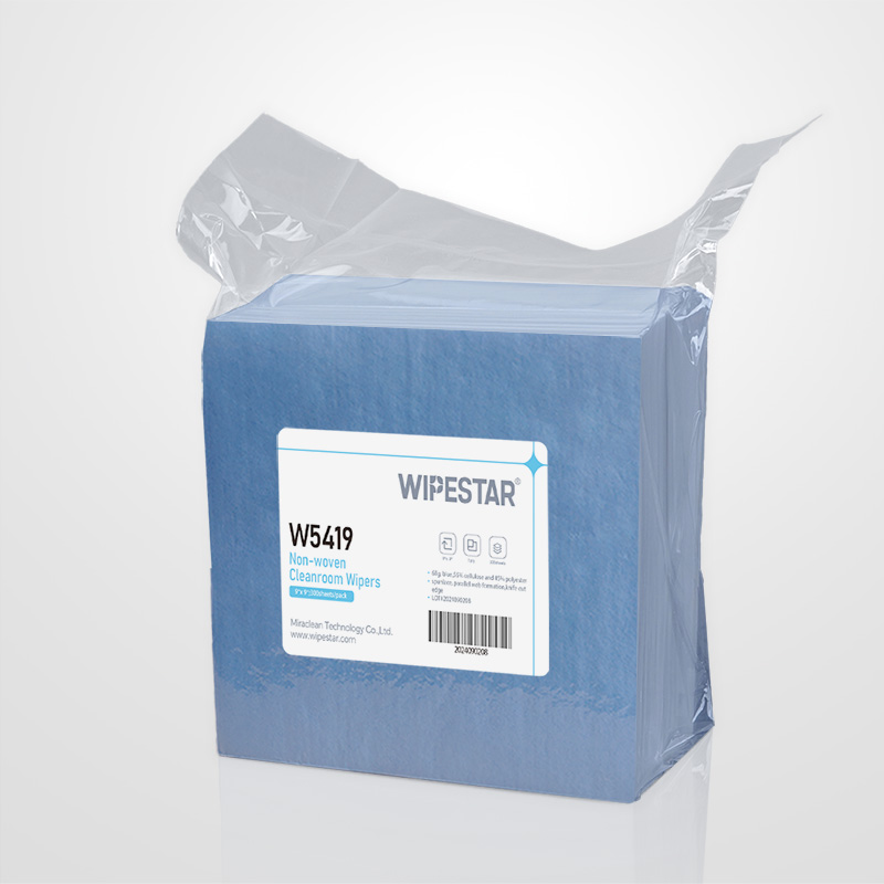
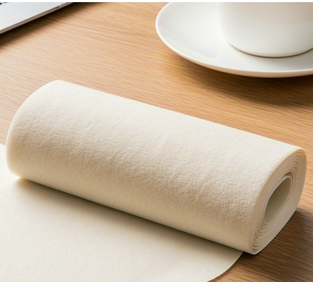
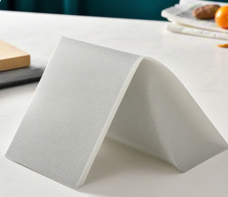
Wipestar W5601 Non-woven Microfiber Cleanroom Wipers offer an optimal cleaning solution for PCB manufacturing environments, combining superior particle capture with excellent durability. Made from a precision blend of 70% polyester and 30% nylon with an 80g/m² weight, these wipers deliver exceptional cleaning performance while minimizing the risk of static discharge and contamination. Their non-woven microfiber construction ensures effective removal of microscopic particles, solder residues, and other contaminants without leaving fibers or creating static charges that could damage sensitive electronic components. Available in 23x23cm and 30x30cm sizes (W5602), these cleanroom-certified wipers are specifically engineered to maintain the stringent cleanliness standards required in PCB manufacturing, making them an ideal choice for both routine maintenance and precision cleaning applications.
RELATED RESOURCES
How Aircraft Wipes Achieve Zero-Contamination Aircraft Engine Cleaning
Wipe star aviation-grade cleaning consumables are manufactured using innovative hydros pinning process, and th......
More
7 Questions on Selecting Ultrafine Dust-Free Wipes: Comparative Analysis of Ultrafine Fiber Cleaning
Comparative analysis of ultra-fine dust-free cloth and ultra-fine dust-free cloth: professional selection guid......
More
The difference between dust-free paper and wiping paper is revealed. 15 years of experience in the f
In the field of industrial cleaning consumables, dust-free paper and wipe paper are two core products often ca......
More
Clean room Wipes Buying Guide: 6 Key Indicators for Professional Purchasers.
Clean Room Dust-Free Wipe Cloth Selection Guide: A Decision Framework for Professional Procurement PersonnelIn......
More
Related Products
Room 101, Building 1, Angeer Factory, No.4, Hetian Road, Shatian Community, Kengzi Street, Pingshan District, Shenzhen, Guangdong, P.R. China 518122
info@wipestar.com
+86-755-89616775
+86-755-89616773
Related Products
RELATED RESOURCES
How Aircraft Wipes Achieve Zero-Contamination Aircraft Engine Cleaning
Wipe star aviation-grade cleaning consumables are manufactured using innovative hydros pinning process, and th.........
More
7 Questions on Selecting Ultrafine Dust-Free Wipes: Comparative Analysis of Ultrafine Fiber Cleaning
Comparative analysis of ultra-fine dust-free cloth and ultra-fine dust-free cloth: professional selection guid.........
More
WIPESTAR
微信官方公众号